- 您现在的位置:买卖IC网 > Sheet目录2006 > LTC2411-1IMS#TRPBF (Linear Technology)IC A/DCONV DIFF INPUT&REF 10MSOP
LTC2411/LTC2411-1
31
APPLICATIO S I FOR ATIO
WU
UU
INPUT SIGNAL FREQUENCY (Hz)
INPUT
NORMAL
MODE
REJECTION
(dB)
2411 F32
0
–10
–20
–30
–40
–50
–60
–70
–80
–90
–100
–110
–120
fN
0
2fN 3fN 4fN 5fN 6fN 7fN 8fN
INPUT SIGNAL FREQUENCY (Hz)
250fN 252fN 254fN 256fN 258fN 260fN 262fN
INPUT
NORMAL
MODE
REJECTION
(dB)
2411 F33
0
–10
–20
–30
–40
–50
–60
–70
–80
–90
–100
–110
–120
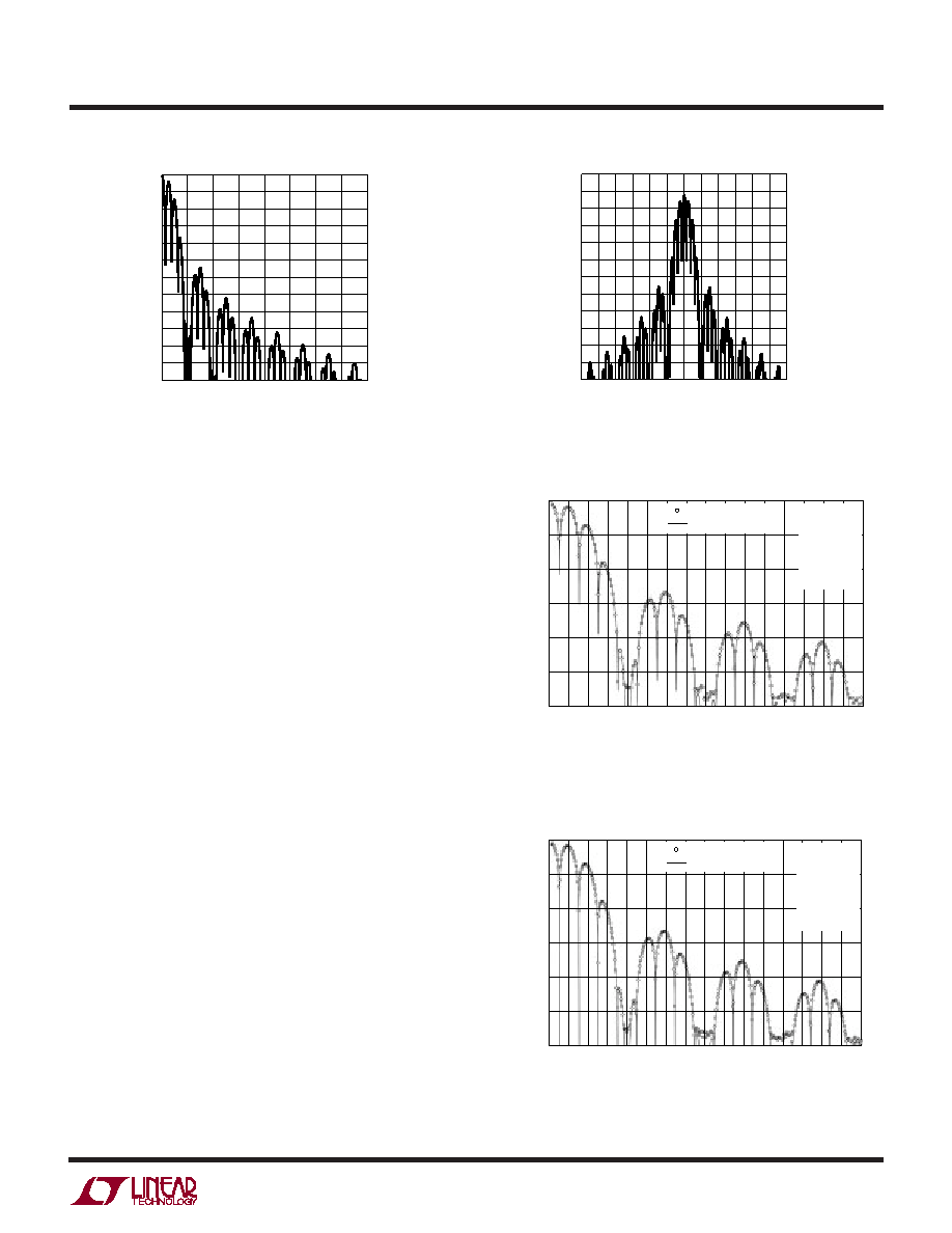
Figure 32. Input Normal Mode Rejection
Figure 33. Input Normal Mode Rejection
INPUT FREQUENCY (Hz)
0
15 30 45 60 75 90 105 120 135 150 165 180 195 210 225 240
NORMAL
MODE
REJECTION
(dB)
2411 F34
0
–20
–40
–60
–80
–100
–120
VCC = 5V
VREF = 5V
VINCM = 2.5V
VIN(P-P) = 5V
FO = GND
TA = 25°C
MEASURED DATA
CALCULATED DATA
INPUT FREQUENCY (Hz)
0
25
50
75
100
125
150
175
200
NORMAL
MODE
REJECTION
(dB)
2411 F35
0
–20
–40
–60
–80
–100
–120
VCC = 5V
VREF = 5V
VINCM = 2.5V
VIN(P-P) = 5V
FO = 5V
TA = 25°C
MEASURED DATA
CALCULATED DATA
Figure 34. Input Normal Mode Rejection
vs Input Frequency (LTC2411)
Figure 35. Input Normal Mode Rejection
vs Input Frequency (LTC2411)
Figure 32 (rejection near DC) and Figure 33 (rejection at
fS = 256fN) where fN represents the notch frequency.
These curves have been derived for the external oscillator
mode but they can be used in all operating modes by
appropriately selecting the fN value.
The user can expect to achieve in practice this level of
performance using the internal oscillator as it is demon-
strated by Figures 34 to 36. Typical measured values of the
normal mode rejection of the LTC2411 operating with an
internal oscillator and a 60Hz notch setting are shown in
Figure 34 superimposed over the theoretical calculated
curve. Similarly, typical measured values of the normal
mode rejection of the LTC2411 operating with an internal
oscillator and a 50Hz notch setting are shown in Figure 35
superimposed over the theoretical calculated curve.
As a result of these remarkable normal mode specifica-
tions, minimal (if any) antialias filtering is required in front
of the LTC2411/LTC2411-1. If passive RC components
are placed in front of the LTC2411/LTC2411-1, the input
dynamic current should be considered (see Input Current
section). In cases where large effective RC time constants
are used, an external buffer amplifier may be required to
minimize the effects of dynamic input current.
Traditional high order delta-sigma modulators, while pro-
viding very good linearity and resolution, suffer from
potential instabilities at large input signal levels. The pro-
prietary architecture used for the LTC2411/LTC2411-1
third order modulator resolves this problem and guaran-
tees a predictable stable behavior at input signal levels of
发布紧急采购,3分钟左右您将得到回复。
相关PDF资料
LTC2418IGN#TRPBF
IC ADC 24BIT DIFF INPUT 28SSOP
LTC2431IMS#TRPBF
IC ADC 20BIT DIFFINPUT/REF10MSOP
LTC2433-1IMS#TRPBF
IC ADC DIFF 16BIT 3WIRE 10-MSOP
LTC2435CGN#TRPBF
IC ADC DIFF I/REF 20BIT 16-SSOP
LTC2442IG#PBF
IC ADC 24BIT 4CH 36-SSOP
LTC2446IUHF#TRPBF
IC ADC 24BIT 8CH HI SPEED 38QFN
LTC2448IUHF#TRPBF
IC ADC 24BIT HI SPEED 38QFN
LTC2451ITS8#TRPBF
IC ADC 16BIT DELTA SIG TSOT23-8
相关代理商/技术参数
LTC2411CMS
功能描述:IC A/D CONV 24BIT MICRPWR 10MSOP RoHS:否 类别:集成电路 (IC) >> 数据采集 - 模数转换器 系列:- 标准包装:1,000 系列:- 位数:16 采样率(每秒):45k 数据接口:串行 转换器数目:2 功率耗散(最大):315mW 电压电源:模拟和数字 工作温度:0°C ~ 70°C 安装类型:表面贴装 封装/外壳:28-SOIC(0.295",7.50mm 宽) 供应商设备封装:28-SOIC W 包装:带卷 (TR) 输入数目和类型:2 个单端,单极
LTC2411CMS#PBF
功能描述:IC A/D CONV 24BIT MICRPWR 10MSOP RoHS:是 类别:集成电路 (IC) >> 数据采集 - 模数转换器 系列:- 标准包装:1 系列:microPOWER™ 位数:8 采样率(每秒):1M 数据接口:串行,SPI? 转换器数目:1 功率耗散(最大):- 电压电源:模拟和数字 工作温度:-40°C ~ 125°C 安装类型:表面贴装 封装/外壳:24-VFQFN 裸露焊盘 供应商设备封装:24-VQFN 裸露焊盘(4x4) 包装:Digi-Reel® 输入数目和类型:8 个单端,单极 产品目录页面:892 (CN2011-ZH PDF) 其它名称:296-25851-6
LTC2411CMS#TR
功能描述:IC A/D CONV 24BIT MICRPWR 10MSOP RoHS:否 类别:集成电路 (IC) >> 数据采集 - 模数转换器 系列:- 标准包装:1,000 系列:- 位数:16 采样率(每秒):45k 数据接口:串行 转换器数目:2 功率耗散(最大):315mW 电压电源:模拟和数字 工作温度:0°C ~ 70°C 安装类型:表面贴装 封装/外壳:28-SOIC(0.295",7.50mm 宽) 供应商设备封装:28-SOIC W 包装:带卷 (TR) 输入数目和类型:2 个单端,单极
LTC2411CMS#TRPBF
功能描述:IC A/D CONV 24BIT MICRPWR 10MSOP RoHS:是 类别:集成电路 (IC) >> 数据采集 - 模数转换器 系列:- 标准包装:1,000 系列:- 位数:16 采样率(每秒):45k 数据接口:串行 转换器数目:2 功率耗散(最大):315mW 电压电源:模拟和数字 工作温度:0°C ~ 70°C 安装类型:表面贴装 封装/外壳:28-SOIC(0.295",7.50mm 宽) 供应商设备封装:28-SOIC W 包装:带卷 (TR) 输入数目和类型:2 个单端,单极
LTC2411IMS
功能描述:IC A/D CONV 24BIT MICRPWR 10MSOP RoHS:否 类别:集成电路 (IC) >> 数据采集 - 模数转换器 系列:- 标准包装:1,000 系列:- 位数:16 采样率(每秒):45k 数据接口:串行 转换器数目:2 功率耗散(最大):315mW 电压电源:模拟和数字 工作温度:0°C ~ 70°C 安装类型:表面贴装 封装/外壳:28-SOIC(0.295",7.50mm 宽) 供应商设备封装:28-SOIC W 包装:带卷 (TR) 输入数目和类型:2 个单端,单极
LTC2411IMS#PBF
功能描述:IC A/D CONV 24BIT MICRPWR 10MSOP RoHS:是 类别:集成电路 (IC) >> 数据采集 - 模数转换器 系列:- 标准包装:1 系列:microPOWER™ 位数:8 采样率(每秒):1M 数据接口:串行,SPI? 转换器数目:1 功率耗散(最大):- 电压电源:模拟和数字 工作温度:-40°C ~ 125°C 安装类型:表面贴装 封装/外壳:24-VFQFN 裸露焊盘 供应商设备封装:24-VQFN 裸露焊盘(4x4) 包装:Digi-Reel® 输入数目和类型:8 个单端,单极 产品目录页面:892 (CN2011-ZH PDF) 其它名称:296-25851-6
LTC2411IMS#TR
功能描述:IC A/D CONV 24BIT MICRPWR 10MSOP RoHS:否 类别:集成电路 (IC) >> 数据采集 - 模数转换器 系列:- 标准包装:1,000 系列:- 位数:16 采样率(每秒):45k 数据接口:串行 转换器数目:2 功率耗散(最大):315mW 电压电源:模拟和数字 工作温度:0°C ~ 70°C 安装类型:表面贴装 封装/外壳:28-SOIC(0.295",7.50mm 宽) 供应商设备封装:28-SOIC W 包装:带卷 (TR) 输入数目和类型:2 个单端,单极
LTC2411IMS#TRPBF
功能描述:IC A/D CONV 24BIT MICRPWR 10MSOP RoHS:是 类别:集成电路 (IC) >> 数据采集 - 模数转换器 系列:- 标准包装:1,000 系列:- 位数:16 采样率(每秒):45k 数据接口:串行 转换器数目:2 功率耗散(最大):315mW 电压电源:模拟和数字 工作温度:0°C ~ 70°C 安装类型:表面贴装 封装/外壳:28-SOIC(0.295",7.50mm 宽) 供应商设备封装:28-SOIC W 包装:带卷 (TR) 输入数目和类型:2 个单端,单极